The leading edge
N5, N3, N2 and beyond — FinFET giving way to gate-all-around nanosheets. The densest logic humanity knows how to build, serving AI accelerators, flagship phones and supercomputers.
 TSMC®
TSMC®
01 / HUMAN SCALE — 10−1 m
Taiwan Semiconductor Manufacturing Company. The pure-play foundry that prints the world’s logic — one wafer, billions of transistors at a time.
02 / THE FAB — 101 m
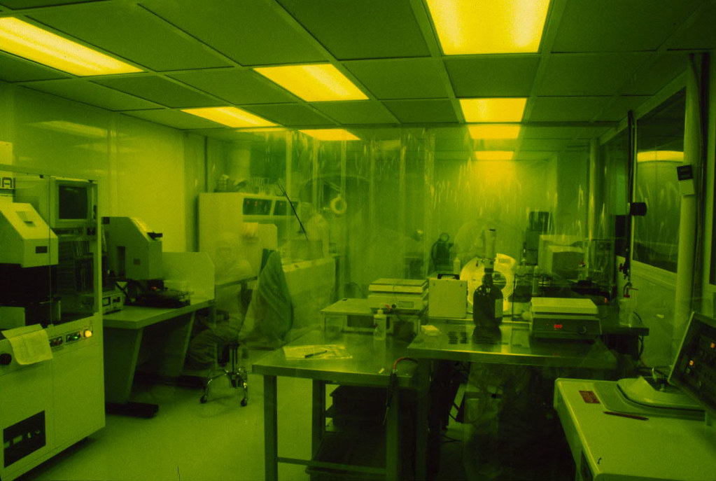
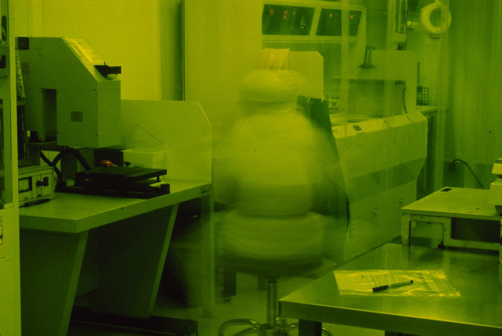
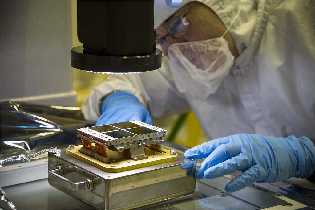
A fab is the most controlled environment humans have ever built. Air scrubbed to ISO Class 1 — thousands of times cleaner than a surgical theatre — bathed in sodium-yellow light, because photoresist cannot see amber.
03 / PROCESS NODES — 10−9 m
A nanometre is the width of ten silicon atoms laid shoulder to shoulder. Each node below is a treaty signed with physics. Scroll — the needle snaps to each milestone.
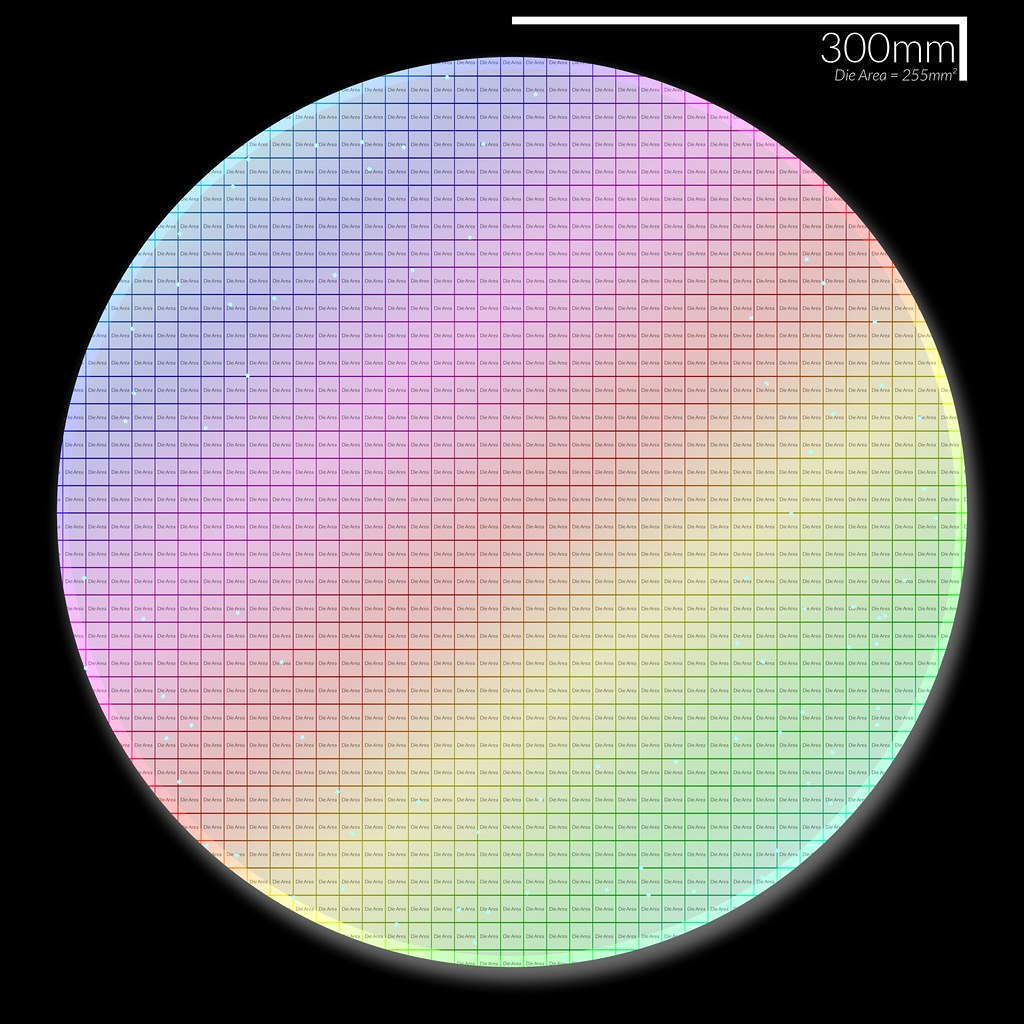
04 / TECHNOLOGY PLATFORMS — 10−6 m
A chip is printed in layers, each one aligned to the last within a nanometre. TSMC’s platforms expose the same way — pass by pass, from transistor to stacked system.
N5, N3, N2 and beyond — FinFET giving way to gate-all-around nanosheets. The densest logic humanity knows how to build, serving AI accelerators, flagship phones and supercomputers.
RF for radios, BCD power management, automotive-grade silicon that must survive fifteen years of engine heat, and CMOS image sensors that gather the world’s light.
CoWoS lays logic and HBM memory side by side on a silicon interposer; InFO fans a die out into a package without a substrate. The AI boom is soldered together here, reticle by reticle.
System on Integrated Chips: wafer-on-wafer hybrid bonding with no bumps at all — copper meeting copper at single-digit-micron pitch. Silicon stacked like storeys of a tower.
05 / THE ECOSYSTEM — 10−3 m
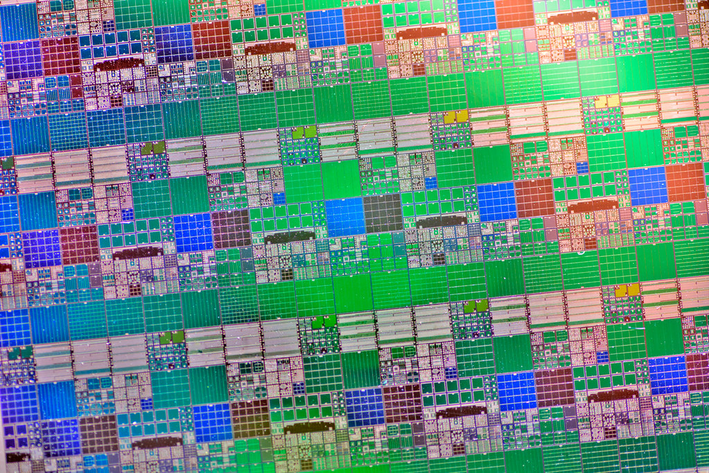
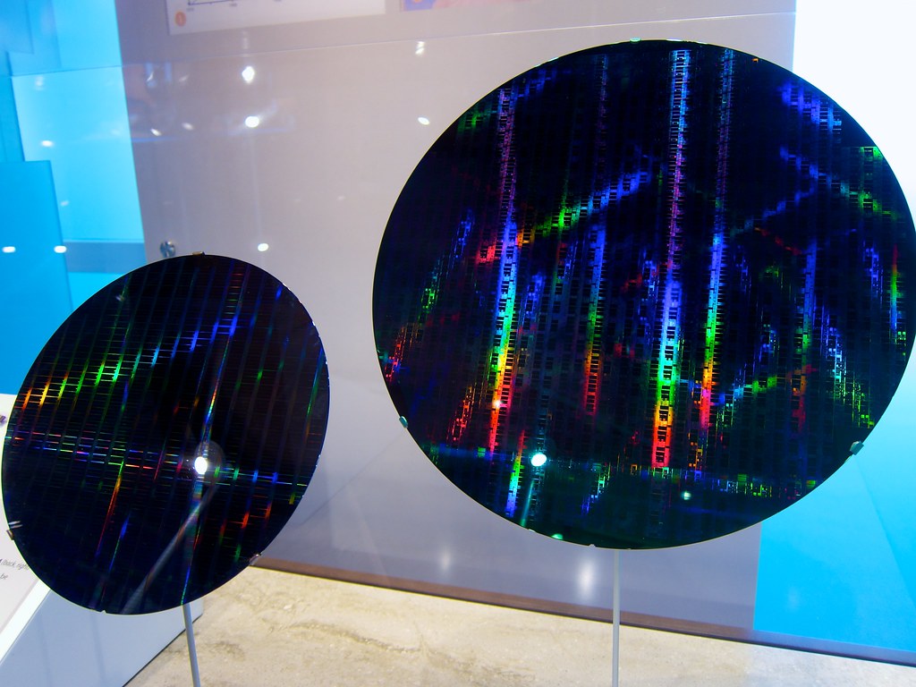
TSMC designs no chips of its own. It is the instrument on which others compose — and nearly every advanced processor on Earth is printed here.
06 / THE RETURN — 103 m
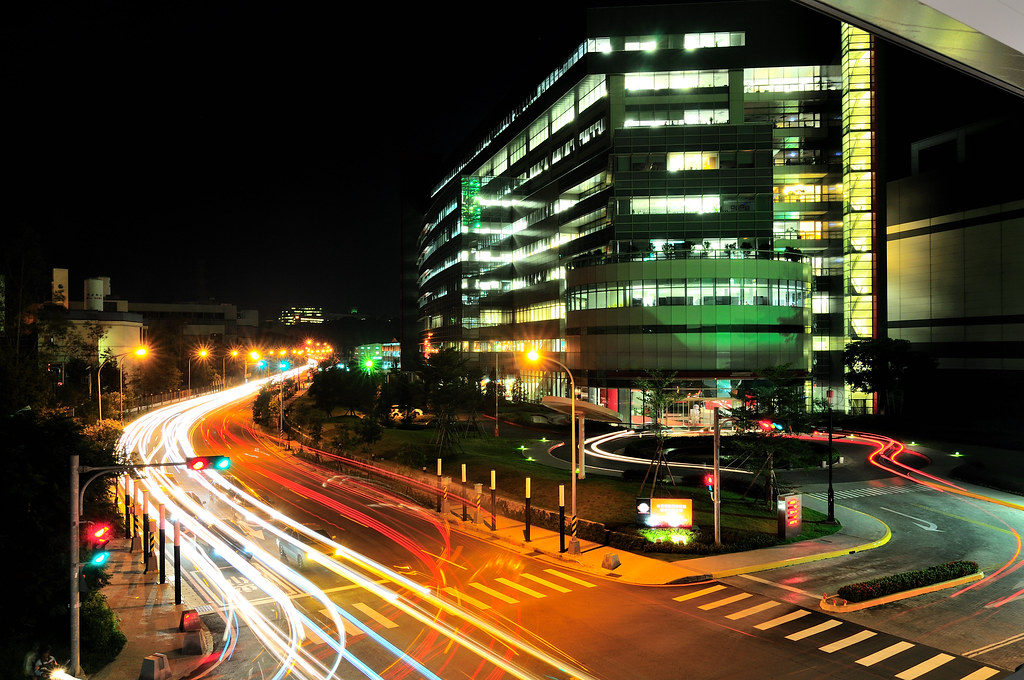
In 1987, in the Hsinchu Science Park, TSMC invented the pure-play foundry: a company that would manufacture anyone’s chip and compete with no one’s design. The idea was doubted. It became the load-bearing wall of the digital age.
Today its GIGAFAB facilities — Fab 12 in Hsinchu, Fab 18 in Tainan, and their sisters across the island — run around the clock, and new fabs rise in Arizona, Kumamoto and Dresden. Taiwan remains the heart of it.
And the craft is learning restraint: TSMC has pledged net-zero emissions by 2050, joined RE100 with a goal of 100% renewable electricity by 2040, and reclaims the great majority of the ultrapure water its fabs drink — fab by fab, the cleanest factories on Earth are becoming the most careful.
BENEATH IT ALL
The silicon lattice constant: 5.431 Å — 0.5431 nm. Every transistor ever printed is furniture arranged on this grid of atoms. The descent ends here. The building does not.